When to choose step stencils?
As technology advances and electronic components become smaller, our methods of fabrication must also advance and improve. One of the many challenges the industry faces today is combining small and large SMT components on a single printed circuit board (PCB). While we strive towards faster and cheaper manufacturing methods, this case scenario presents a big challenge namely applying the right volume of solder paste.
If you’re not familiar with the soldering process of SMT components on a circuit board, it is very simple yet challenging. Today the manufacturing process that dominates fast and reliable PCB manufacturing is using a SMT stencil to print solder paste on the PCB. SMT stencils have very small cut-outs (usually called apertures) for each point of union between the PCB and the components, these cut-outs are in the range of microns. After the solder paste is carefully applied and the SMT components are placed on the SMT pads of the board, the PCB is placed in a reflow oven. When heated up, the paste melts (reflows) and solders the components to the board.
So where’s the challenge? Not all SMT components are created equal. While there are large components such as like .5mm QFP’s, there are new micro components such as .3 mm CSP and uBGA devices. These components require much less solder paste in order to be soldered correctly on the board.
HOW MUCH SOLDER PASTE SHOULD BE APPLIED?
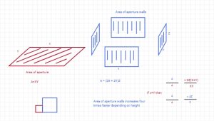
In order to know how much paste should be applied engineers have developed what is called Area-Ratio. The Area-Ratio is the ratio between the area of the aperture (where solder paste will be deposited) and the height/thickness of the stencil, which can be anywhere from 50 microns up to 500 microns.
Area ratio = Aperture area / Area of aperture walls
Stencils Unlimited uses the IPC-7525B guideline with a minimum recommended 0.66 area ratio. So how do we keep our ratios above 0.66 when we have multiple components? With step stencils.
Step stencils have with different levels, this means that we can have multiple thicknesses within the sameIf you take a look at the Area Ratio equation, for a very thick stencil, the area of aperture walls will increase (depends on the Z coordinate) while the aperture area (depends on X,Y coordinates) will remain the same.
This means that if we have very thick stencils with small components, the area ratio will be under 0.66 for small components. We use step stencils to reduce the thickness thus having a smaller denominator and increasing this ratio to a minimum 0.66.
There are many different ways to create step stencils, plese refer to Manufacturing Step Stencils. They’re basically four methods: high speed machining, electroforming, laser welding and chemical etching.
WHY WOULD WE CHOOSE STEP STENCILS?
You can certainly use different stencils with different thicknesses on the same board applying each volume separately until you achieve your desired result. However this method is prone to mistakes, if done incorrectly you could alter the solder paste already applied on the printed circuit board. This method is also more expensive as you may require to fabricate multiple stencils and it will take more manufacturing time as it involves multiple runs.
If you want to fabricate printed circuit boards with multiple paste volumes as quickly and efficiently as possible, step stencils are the way to go. They will reduce costs, improve productivity and apply the correct volume of solder paste reliably.
You can order a step stencil directly from our website.