Stencils Unlimited
Step stencils, often called multi-level stencils, offer much more flexibility when it comes to solder paste volume deposits. They fundamentally control the volume of solder paste needed by changing the stencil thickness needed for small and large SMT components within the same stencil.
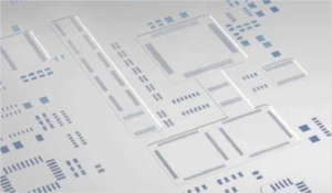
Figure 1
Step Stencil
The most common step stencils are step-up and step-down stencils. When it comes to PCB Assembly, the type of step you should use will depend on the ratio of small SMT components to large SMT components. If the PCB uses mostly large components then a step-down stencil would be recommended to reduce the solder paste volume needed for small components.
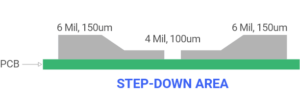
Figure 2
If the PCB uses mostly small components then a step-up stencil is the most adequate to increase the volume of solder paste for the large components.
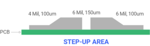
Figure 3
There are four methods to manufacture step stencils: photo-chemical etching, high speed micro machining, additive laser welding and electroforming.
PHOTO-CHEMICAL ETCHING
To create steps using this method, the stencil is bathed with a chemical that removes material to achieve the desired thickness. The steps are created using a special photoresist laminated sheet which is applied to the metal sheet prior to etching. Before applying the chemical, the outline of each section that requires a different thickness is printed on the photoresist, which then allows the chemical to only degrade these sections of the sheet. After removing the photoresist sheet, we’re left with a metal sheet with different thickness areas. We then move our metal sheet to the laser cut and create our step-stencil.
HIGH SPEED MICRO-MACHINING
Micro machining removes material with a high speed CNC milling drill. It’s programmed to remove material from our metal sheet with high precision creating the areas which need different thickness. Just like photo-chemical etching, it is an abrasive process, however, it yields the highest accuracy for positioning.
ADDITIVE LASER WELDING
In contrast to high-speed micro-machining and photo-chemical etching, this technique adds material instead of removing it. If our stencil requires 0.004” thickness for most SMT components and 0.008” for larger components, we proceed by combining two sheets of each thickness. Using the thinner sheet as base, the sections which need to be thicker are cut out from the former sheet. Then the “negative” or missing piece is cut out from the thicker sheet. After replacing each section with its exact thicker copy, they’re then welded by laser together. The result is one foil with different thickness sections.
ELECTROFORMING
This method consists of adding layers on top of each other to create steps. This must be done with extreme accuracy to avoid placing steps over a pad or edges too close to a pad. The recommended distance is at least 0.5 mm from the edge of a step to a pad. This is the least used method as it requires a lot of effort and doesn’t necessarily bring the best results.
Our goal with stencil design should always be to apply the exact amount of solder paste needed for each component. Step stencils give us a great design solution to an increasingly complex market with mixed components while achieving results faster than traditional methods, such as using several different stencils. While there are different ways to create a multi-level stencil, we should always use the most effortless method to save time and resources. Other subsequent benefits include coplanarity between components with different heights, and completely gasketing the PCB with the stencil as the gap between the apertures and pads is eliminated.
Stencils Unlimited can provide step stencils with high precision milling for your PCB, our team has optimized design to precisely deliver the optimum amount of solder paste. You can order a step.